• Skip to content
  • Skip to primary sidebar

Dr. Senad Bulja, PhD, FIET, SMIEEE

  • Home
  • Researches
  • Workshops
  • Patents
  • Products
  • Tutorials
  • Solutions
  • Services
You are here: Home / Patents / Electroactive material – Controlled smart surface

Electroactive material – Controlled smart surface

15/03/2023 by Dr. Senad Bulja Leave a Comment

Publication number: 20210313390
Type: Application
Filed: Apr 1, 2020
Publication Date: Oct 7, 2021
Applicant: Nokia Technologies OY (Espoo)
Inventors: Senad BULJA (Dublin), Dirk WIEGNER (Schwaikheim), Wolfgang TEMPL (Sersheim), Rose F KOPF (Green Brook, NJ)
Application Number: 16/837,717

Abstract: The main idea of the invention is to propose the use of Electro-Active (EA) materials for the realization of Intelligent Surfaces (IS). For this purpose, a basic structure, shown in Fig. 1 is proposed. The proposed solution consists of NxN individual elements (4 x 4 dielectric tiles and 5 x 5 EA tiles in the depicted figure). By activating the EA material, the dielectric tiles become mobile in the x and y directions, resulting in the surface whose dielectric permittivity is a function of the spatial position and, due to the nature of EA materials, controllable. By having a surface whose dielectric permittivity, as a function of the spatial coordinates is controllable, one is able to perform a variety of mathematical operations, including differentiation, integration, convolution and more, as indicated earlier. Furthermore, by properly manipulating the dielectric permittivity as a function of the spatial coordinates one is able to even directly modulate the input signal. This can be done by applying the message signal to the bias lines of the proposed surface of Fig. 1.
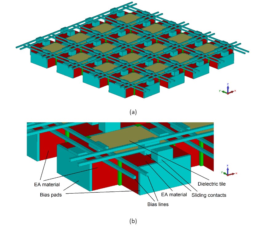
Fig. 1. Proposed EA-based smart surface. (a) perspective view of single layer smart surface showing all elements, and (b) perspective view showing individual layers in detail

Filed Under: Patents Tagged With: 5G filters, 6G filters, Electro-Active Intelligent Surface

Reader Interactions

Leave a Reply Cancel reply

Your email address will not be published. Required fields are marked *

Primary Sidebar

Profile & Bio

Senad Bulja, Ph.D., FIET, SMIEEE 

  1. Dr Bulja’s profile
  2. Email : contact@drbulja.com

PROFESSIONAL Profile

  • Accomplished career of over 19 years demonstrating consistent success as a Researcher, Leader and Mentor in the Wireless industry research environment.
  • Excellent Scientific contributions in the field of RF, EMC and telecommunications with 4 Nature Journal publications and over 70 peer-reviewed articles and conference papers
  • Strong leadership skills demonstrated by leading Ph.D. level educated cross-continental and cross-departmental teams to successful project execution.  
  • Proven Strategic Business Impact – introduced own developed technology into Nokia’s future technology roadmap (RF filters) and business transfer of the smart surface technology. 
  • Creative, internationally awarded and well-driven inventor with over 70 filed patents in the area of hardware for Radio Frequency (RF), Wireless Sensor Networks (WSN), Internet of Things (IoT) and wireless systems architectures. E.g. Nokia patent award entitled: “A top inventor in implementation patent first filings”, 2020.
  • Significant contribution in the identification of high revenue IP assets and leadership on the creation of Nokia’s patent portfolio roadmap. 

 
[event_submit_caldera id='CF63b4de7ecb50c' category='dat_hang_chan_trang' action='submit' label='oder_footer']

Copyright © 2026 · Genesis Framework · WordPress · Log in